FSM 413C2C
全自動晶圓多功能測量系統

Fully Automated High Resolution Substrate Thickness, Via Depth, Warp, & Bow and TTV Mapper

» Measures Substrate Thickness in Multiple Layers using Non-contact

Optical System

» High Precision XY Stage (0.5m)

» Robotic Handling system

» Programmable Data Points

» Lateral Data

» Measures Silicon via Depth with Microscope option

» Excellent Repeatability & Reproducibility

» Pattern Recognition Function


  • FSM 413

    This FSM 413 Echoprobe(TM) sensor used patent pending Infrared (IR) Interferometric Technique which provides a direct and accurate map of thick to ultrathin wafer measurement of substrate thickness, and thickness varia tion (1TV).

    Several materials transparent to in IR beam, such as Is, GaAs, InP, SiC, Glass, Quartz and many polymers spot, (smaller spot sizes are available). Using a Single probe system, substrate thickness of conventional wafers with patterns, tapes, bumps or bonded wafers mounted on carriers can be determined with high precision and accuracy.

    When configured as a Dual probe system, the FSM413 also provides measurements of total thickness of the wafer including substrate thickness and the patterned height thickness. Options are available to measure the wafer warp, trench depth and cia holes, including high aspect ration trenches and vias in MEMs type applications. Various specialized MEMs applications including Membrane Metrology and Bump Height metrology are also available.

  • SPECIFICATIONS

    Technique: Non-contact IR interferometry, Single or Dual
               Probe.
    Wafer size: 50, 70, 100, 200, 300 mm.
    Customized wafer sizes also available
    Substrate : Si, GaAS, InP, Quartz, Glass, SiC, Sapphire
    Thickness range: 30-70pm for Single Probe measurement
               1 up to 3 mm Dual Probe (total thickness)
               measurement
    Wafer loading: Manual
    Measurement mode: Semi automated with precision x-y
               stage
    RESOIUHOH (Display): 0.01µm
    Repeatablllty. 0.1µm (1 sigma) in Single Probe
                   1.8µm (1 sigma) in Dual Probe Mode
    Accuracy : 0.5pm (1 sigma)
    Measurement points: Programmable
    Substrate thickness results: TTV, Mean, Maximum, Minimum
                SiDev, 2D and 3D Color Maps


OPTIONS

Warp Measurement range: Contact Honyang for details

Warp Repeatability: Contact Honyang for details

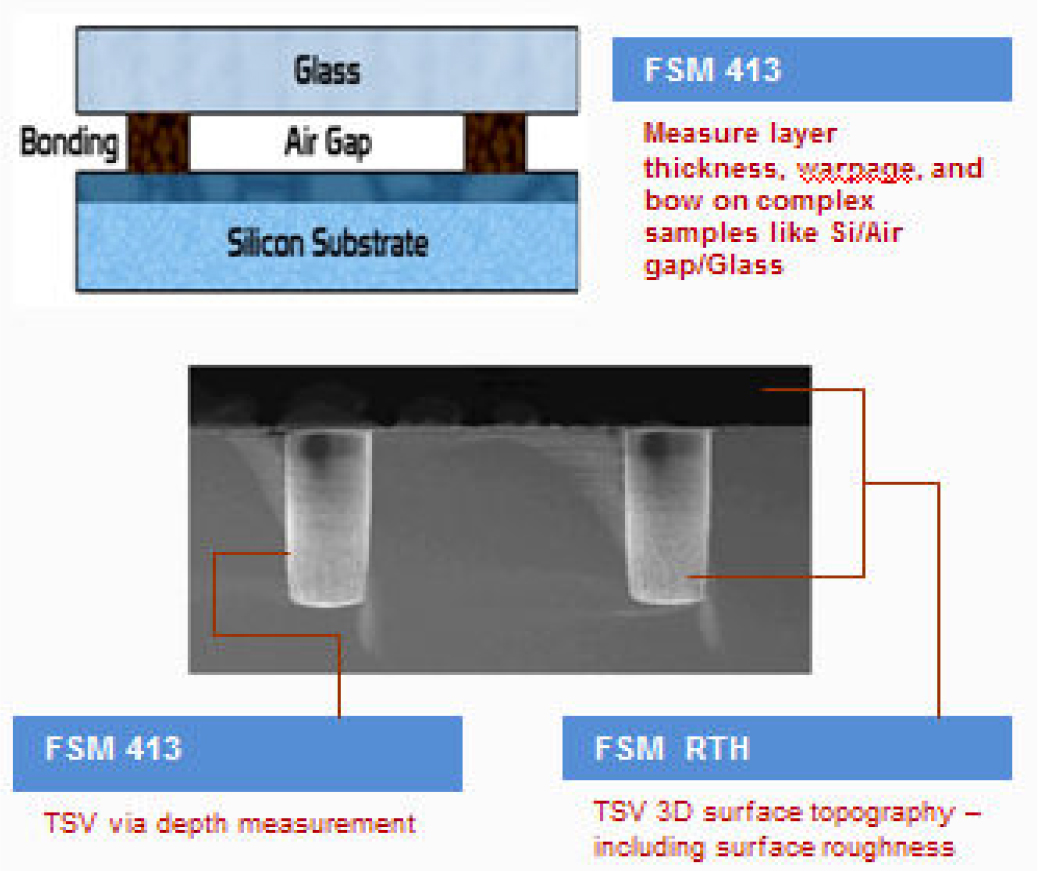
Surface Roughness: RMS range of 20-1000 A

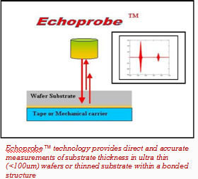
Trench Depth Measurements: Contact Honyang for details

Polymide Film and Epoxy Thickness Measurements : Contact Honyang for details

Bump Height Metrology: Contact Honyang for details

Dimension (Main Equipment) :413 - 200: 26"(W) x 36"(D) x 56"(H)

                            413 - 300: 32"(W) x 46"(D) x 86"(H)

Weight (Gross): 500Ibs

Power: 110 or 220 VAC, 50/60 HZ, Single Phase, 3 wire

Vacuum Required: 100 mm Hg

*Surface must be smooth (generally roughness <0.1µm, RMS)

**on 150µm thick unpatterned double sided polished undoped Si wafer

OTHER APPLICATIONS

Trench Depth Measurements

Surface Roughness

Thin Film Thickness Measurement

Epoxy Thickness Measurement

Warp Measurement

Bump Helgnt Measurement