弘揚環球科技
Honyang Global Technology CO., LTD

Honyang Global Technology CO., LTD
特性:
應用在納米機械測試中的創新研究
我們提供為學術界和工業界的高精度納米壓痕技術。
我們提供納米壓痕技術平臺是相容現地使用的掃描電子顯微鏡
(SEM),也使用和一般環境,通用的其他相關設備相同,例如同步輻射光束線或光學顯微鏡,因此在提供無與倫比的靈活性、 準確性和真實臨場的納米力學測試,皆可對於繁多不同的種類材料應用.
Characteristic:
Enabling innovative research in nano-mechanical testing.
We offers high-precision nanoindentation technology for academia and industry.
Our Nanoindentation Platform is compatible for in-situ use with Scanning Electron Microscopes (SEM), and also for in-air use with for example Synchrotron beamlines or light microscopes, thus providing unparalleled flexibility, accuracy and true in-situ nanomechanical testing of a wide variety of materials for different applications.
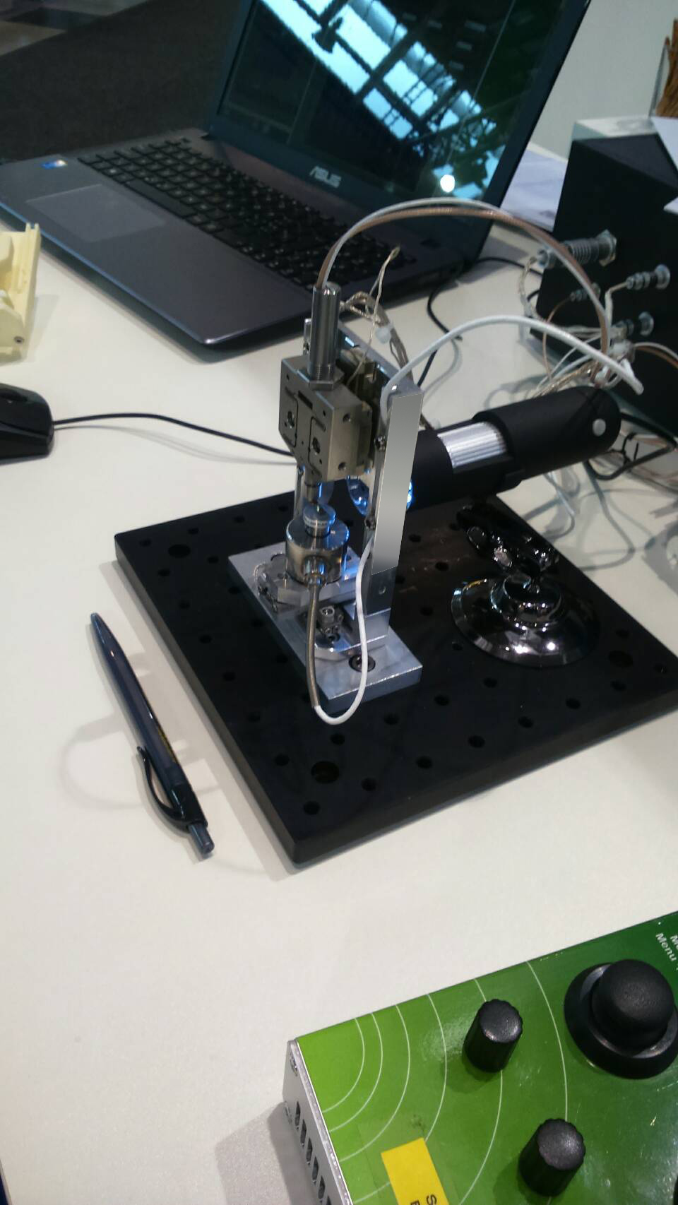
| Indenter main specification (in-SEM and in-air) |
| · Compact size 16.6cm * 6.5 cm * 46cm |
| · Indentation load:Oe5N ( 4μN RMS Noise@200 Hz, axial compliance: 4.7 μm ∕ N ) (optional up to 1.5N) |
| · Maximum indention depth: 35μm (+/- 1.8 nm resolution) |
| · XY closed loop sample micro-positioning system. 10 * 10 mm sample covering area (2 nm resolution) |
| · 22 mm range positioning system in Z-axis for easy setup of sample height ( 2 nm resolution) |
| . High-vacuum compatible components (IOe-6mbar) |
| · Weight approx. 500g |
| . National InstrumentsTM control electronics and LabViewTM, control software AMICS |